UniversityWafer announces new supply silicon-on-insulator substrates
The company seeks to empower photonics researchers and support prototyping with its 220 nm device layer SOI, which customers can buy in quantities as small as a single wafer or diced pieces
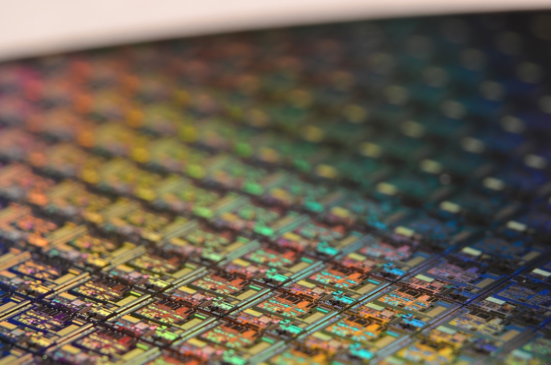
UniversityWafer, a provider of advanced semiconductor materials, has announced that their new supply silicon-on-insulator (SOI) substrates, which it says are poised to redefine the landscape of on-chip photonics research. According to the company, researchers can now buy as few as one thin device layer SOI wafer, or even diced pieces, ensuring that even researchers with limited budgets can continue their project with high-quality SOI at a low price. UniversityWafer says its inventory of 220 nanometre device layer SOI, sets a new standard for precision and performance in photonics applications.
Photonics, the science and technology of generating, controlling, and detecting photons, lies at the heart of numerous cutting-edge technologies, including telecommunications, quantum computing, and biomedical imaging. The demand for high-performance photonics devices continues to surge, driving the need for innovative materials that can deliver superior functionality at the nanoscale.
To address this demand, UniversityWafer says its SOI substrates are engineered to empower researchers and engineers with unprecedented control and versatility in on-chip photonics experimentation. By integrating a 220 nanometre device layer into its SOI substrates, the company aims to enable researchers to explore the full potential of photonics at the microscale, unlocking new possibilities for optical communication, sensing, and computing.
“Our SOI substrates with a 220 nanometre device layer represent a paradigm shift in the field of photonics,” says Christian Baker, founder and CEO of UniversityWafer. “With this ultra-thin and highly uniform platform, researchers can fabricate and characterise a diverse range of photonic devices with unparalleled precision and efficiency. Whether it's waveguides, modulators, or photodetectors, our SOI substrates provide a robust foundation for pushing the boundaries of on-chip photonics.”
The company adds that the efficacy of 220 nm SOI substrates has been underscored by recent research findings published in leading academic journals. For example, in a study published in Nature Photonics, researchers demonstrated the exceptional performance of photonic devices fabricated on 220 nm SOI substrates, showcasing their potential for high-speed optical interconnects and quantum communication systems. Similarly, a paper in Optics Express showcased the versatility of these substrates for integrated photonics applications, highlighting their low optical loss and high optical confinement properties.
UniversityWafer adds that the impact of its SOI substrates extends to industry, by providing a robust platform for prototyping and testing photonic devices, and thus empowering companies to accelerate the development of next-generation optical technologies, from datacentres to medical devices.
The company says it is also committed to fostering collaboration and knowledge exchange within the photonics community, offering support and resources to facilitate breakthroughs in on-chip photonics research through partnerships with leading research institutions and industry players.