Giving photons a sense of direction for better LEDs
UC Santa Barbara researchers show how metasurface design methods can make LED light act more like lasers
UC Santa Barbara researchers continue to push the boundaries of LED design a little further with a new method that could pave the way toward more efficient and versatile LED display and lighting technology.
In a paper published in Nature Photonics, UCSB electrical and computer engineering professor Jonathan Schuller and collaborators describe this new approach, which could allow a wide variety of LED devices - from virtual reality headsets to automotive lighting - to become more sophisticated and sleeker at the same time.
"What we showed is a new kind of photonic architecture that not only allows you to extract more photons, but also to direct them where you want," said Schuller. This improved performance, he explained, is achieved without the external packaging components that are often used to manipulate the light emitted by LEDs.
Light in LEDs is generated in the semiconductor material when excited, negatively charged electrons traveling along the semiconductor's crystal lattice meet positively-charged holes (an absence of electrons) and transition to a lower state of energy, releasing a photon along the way. Over the course of their measurements, the researchers found that a significant amount of these photons were being generated but were not making it out of the LED.
"We realised that if you looked at the angular distribution of the emitted photon before patterning, it tended to peak at a certain direction that would normally be trapped within the LED structure," Schuller said. "And so we realised that you could design around that normally trapped light using traditional metasurface concepts."
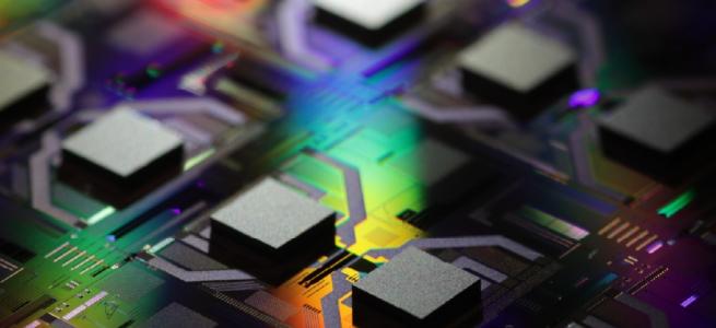
The design they settled upon consists of an array of 1.45-micrometer long GaN nanorods on a sapphire substrate, in which quantum wells of InGaN were embedded, to confine electrons and holes and thus emit light. In addition to allowing more light to leave the semiconductor structure, the process polarises the light, which co-lead author Prasad Iyer said, "is critical for a lot of applications."
Nanoscale Antennae
The idea for the project came to Iyer a couple of years ago as he was completing his doctorate in Schuller's lab, where the research is focused on photonics technology and optical phenomena at subwavelength scales. Metasurfaces - engineered surfaces with nanoscale features that interact with light - were the focus of his research.
"A metasurface is essentially a subwavelength array of antennas," said Iyer, who previously was researching how to steer laser beams with metasurfaces. He understood that typical metasurfaces rely on the highly directional properties of the incoming laser beam to produce a highly directed outgoing beam.
LEDs, on the other hand, emit spontaneous light, as opposed to the laser's stimulated, coherent light.
"Spontaneous emission samples all the possible ways the photon is allowed to go," Schuller explained, so the light appears as a spray of photons traveling in all possible directions. The question was could they, through careful nanoscale design and fabrication of the semiconductor surface, herd the generated photons in a desired direction?
"People have done patterning of LEDs previously," Iyer said, but those efforts invariably split the into multiple directions, with low efficiency. "Nobody had engineered a way to control the emission of light from an LED into a single direction."
Right Place, Right Time
It was a puzzle that would not have found a solution, Iyer said, without the help of a team of expert collaborators. GaN is exceptionally difficult to work with and requires specialized processes to make high-quality crystals. Only a few places in the world have the expertise to fabricate the material in such exacting design.
UC Santa Barbara, home to the Solid State Lighting and Energy Electronics Center (SSLEEC), is one of those places, say the researchers. With the expertise at SSLEEC and the campus's world-class nanofabrication facility, the researchers designed and patterned the semiconductor surface to adapt the metasurface concept for spontaneous light emission.
"We were very fortunate to collaborate with the world experts in making these things," Schuller said.
'Unidirectional luminescence from InGaN/GaN quantum-well metasurfaces' by Prasad P. Iyer et al; Nature Photonics 01 June (2020)