Quality challenges data center PIC ascendency

PIC Magazine Technical Editor Mark Andrews recently continued a conversation with Facebook Manufacturing Quality Engineer (Optics) Vincent Zeng that began shortly after Zeng spoke at PIC International 2018 in Brussels, Belgium in April. Zeng reported that while Facebook and other major optical data component end users continue to put their faith in the evolution of next-generation transceivers to satisfy escalating requirements, the transition to advanced PIC-based 100G devices has not been without challenges.
Zeng and his Facebook colleagues reported high levels of rejected devices compared to prior generations of optical devices and what they describe as "˜DOA' products"”devices that are essentially Dead on Arrival because they fail within two months of commencing operation. Tighter quality controls, process automation and more openness to sharing production techniques will not only speed the transition to next-generation PIC solutions, he asserted, but are important to PICs realizing their potential in data center applications.
Zeng's remarks in Brussels no doubt caught some PIC International attendees off-guard. Others already realized that issues surrounding the implementation of new PIC-powered 100G transceivers in a data center's highly complex operations present many issues as well as opportunities.
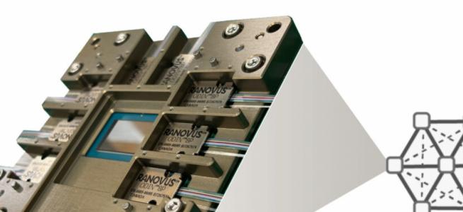
After working in quality engineering field for 12 years, almost 3 years at Facebook, Zeng has seen generations of products pass under his group's watchful eyes. The latest PIC-based solutions have experienced unusually elevated level of rejects from the beginning of large deployments of the products. This is due to several functionality and process control issues stemming in part from the fact that the relatively new photonics integration industry is still striving to attain the levels of quality control and automation that other semiconductor manufacturers have adopted as standard operating procedures (SOP). Photonic integrated circuits are striving to grow beyond their "˜lab-to-fab' roots.
Zeng noted that while the overall semiconductor industry has honed and refined its process control, automation and testing environments based upon five decades' experience, the processes required to consistently manufacture high quality photonic integrated circuits with high yield are in comparison just getting off the ground. The photonics devices normally require unique packaging; new PICs offer standardized process and preserves die-level performance while simultaneously providing necessary fiber and intra-center system connectivity. In some cases, manufacturers are integrating optics and electronics. Adding to the challenge is the need to integrate lasers (typically indium phosphide-based) into a different material system for IC (silicon-based material) while managing RF issues as well as providing important optical coupling alignment.
Zeng and Facebook colleagues Katharine Schmidtke and Edward Galley said following PIC International that a way to "˜distill' their overall concerns as simply as possible is the recommendation that designers and manufacturers need to focus up front on "˜how to make it (pics) work' with consistency and high quality.
"For most photonic suppliers, "how to make it work" is their challenge when they try to deliver advanced photonic products. The 100G CWDM4 product was a good example back two to three years ago when they were still in the early phases of development/production. After the mass production phase, unstable and more importantly, unpredictable yield impacted the deployment schedule and plans at major data center operators."
"As a result, backward compatibility (called 40G/100G dual-modes) was required in the early stage of 100G CWDM4 deployment. The unpredictable yield that we have seen comes from a device burn-in process for the 25G DFB lasers that was not mature. Each laser supplier has a different process embedded that require different burn-in conditions depending on which module supplier would assemble the laser die into the final products. We believe that a manufacturing screening process (designed) to avoid what could be called infant mortality failure was the main reason for unpredictable and unstable yields across different processes and factories."
"Another fact that brings the scalability down is the individual supplier carries its own "˜secret recipe' for its products. There is no interoperability from one supplier's key optical sub assembly (OSA) to another supplier's packaged module. Most of these secret recipes are purely process oriented. This ultimately applies to requirements for several types of capital equipment for production," he noted.
While Zeng attributes many of the product failures he and his colleagues have observed to manufacturing process issues and variability between manufacturers, the majority of issues are laser-related failures. He noted that behind laser issues, Facebook quality managers have also seen PCBA or receiver related failures, and a small amount of miscellaneous issues.
"During these (past) two years' actual deployment of the 100G CWDM4 optics at our data centers, we identified almost all failures directly coming from laser related (laser die or TOSA) and the rest comes from module level handling, even if the overall module performance meets our expectation. We also identified all these failures come from what we call DOAs-- dead on arrival-- meaning they fail within two months after power-on. After failure analysis of those defects, we identified the process (excursions) at the factory were root causes. Those include electronic discharge events to the ICs and laser dies as products are handled during the packaging process, optical handling contaminations to key optical components and the improper process (excursions) without solid test steps."
"Also, we are facing tremendous challenges in process control to avoid the infant mortality failures from factory both on the wafer level and module level. We believe high activation energy related failures mainly come from wafer and laser process issues and low activation energy related failures mainly come from the optical package. To find the proper screening process at wafer level and module level indeed is still a challenge for the photonic industry. Without consistent processes in place, it is even harder to develop a solid screening process," Zeng explained.
To better understand the issues surrounding the ways that new PIC devices are introduced into data center operations, Zeng said it is best to consider three major categories of pluggable transceivers: wafer level, component forming and module forming.
"With current InP wafer fabrication processes, the conventional yield management tool has not been widely used. The defect control for each step has not been a standard (adhered to) across different suppliers/vendors. Post Burn-In process (steps) are widely used, instead of during the different fabrication process. For the wafer level, PICs should follow the IC industry's yield management standards. We need to define the quantitative criteria for the defects and contaminations for each fabrication process: the defect kind, the defect size, the location of the defect, and the critical dimension control. In short, in-situ wafer level tests (need to) be fully characterized before this wafer moves to its next process step. To achieve that goal, the proper equipment will be needed. Additionally, IC industry standards need to be applied; PIC designers will need to pay attention to the optical performance in time control such as the refractive index control during fabrication," he said.

Figure 1. Wafer Level Management Evolution for PIC
Based on the defective devices that Zeng and his other quality engineers have observed, PIC manufacturers could benefit from more and better characterization on the wafer level to avoid significant discrepancies between the performance of a device at wafer level as unpackaged die, and at the module level once the device has been packaged. He appreciates the challenges that manufacturers face since PIC devices and optical components in general typically see performance variations depending on changes in temperature, humidity and pressure to a greater degree than other component families. Quality managers see variabilities that often tie back to packaging or handling issues focused on three main areas: varying materials used in devices that react differently to environmental conditions that still need to keep performance and reliability high; optical coupling including V-groove arrays are experiencing alignment issues especially at multiple fiber connection points; and the sensitivity of optical components to stress and indirect refractive index. Device reliability is ultimately impacted through these potential fault points.

Figure 2. PIC Packaging Challenges
"We believe ultimately that consistent process control realized (through) less human contact with components and more automation will reduce process related failures. This requirement will be applied to the wafer level process as well as the photonic package level," Zeng noted, adding that manufacturers are already responding. "We are consistently seeing monthly manufacturing yield and field quality performance improvements after we introduce more and more automation into packaging process. Tight and consistent screening for defects on the wafer level also helps to increase yield."
"From what we have learned, more consistent process (steps) with less human handling errors results in higher quality of the photonic device. Co-packaged optics solutions will eventually help to meet those challenges. Co-packaged optics will integrate (the) ASIC and optics on the wafer level and dramatically reduce the integration steps required during packaging processes. Wafer level integration will aid quality because we will have many fewer discrete optical components; we will fully utilize current IC CMOS process standards to strictly control the building block process. In real application fields like in data centers, the number of pluggable devices will be dramatically reduced with deployment of the co-packaged optics switches," he explained.
Despite the challenges being experienced as photonic integrated circuits (PICs) enter data center operations, the benefits of the PIC revolution such as reduced complexity, size and lower power consumption are greatly needed in data centers and along other infrastructure nexus points. Zeng reported that existing suppliers are stepping up and making changes, noting that, ""¦we are meeting with our suppliers intensively." And while he expects that suppliers and manufacturers will continue to use proprietary "˜recipes' for device fabrication, applying common standards like those used successfully in mainstream silicon and III-V device manufacturing will only speed what everyone hopes will be a successful transition to next generation high speed PIC transceivers.
"Volume demand is really the driving force for PIC, currently and for the foreseeable future. Big data centers will continue to play as the main force. The demands of Big Data are pushing this process; PIC (manufacturers) will respond to focus on (their) process development from the wafer level and prepare for another huge wave to come. The PIC era will arrive with denser optical electrical integration and more application and usage will be defined"¦The negatives we have experienced so far have impacted the scaled deployment within limited opening windows, but we will succeed. Manufacturers can be enablers of quicker, successful PIC device adoption by acting on our recommendations."